 |
Dynamic Mapping System (DMS) and DMS Status PCB |
As part of familiarising myself with the operation of the CPU I needed to know how extended memory is accessed. Also when the system software is loaded from a tape the system must know The 2105A CPU used in the Keyboard and Control Unit (HP5443A) is part of the 21MX series of CPUs made by HP. This processor has a 16 bit data bus and has 15 bit address bus so only 32k words of memory can be directly addressed by the processor.
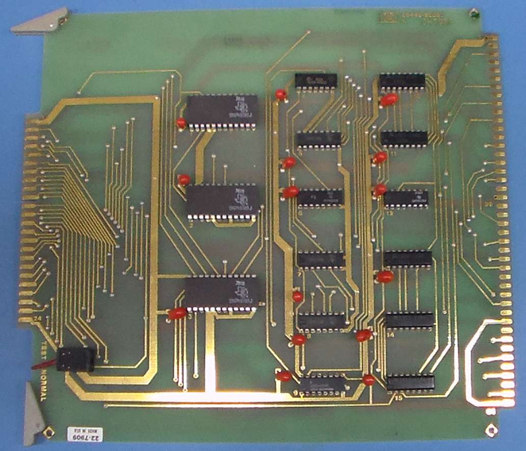
Before the 5420A and 5423A systems were designed HP had already designed memory expansion systems such as the HP 12731A which allows the mapping of up to 1M word of memory into the 32k word address space of the processor. For the 5420A/23A systems a simplified version the 12731A was implemented, the Dynamic Mapping System Board (DMSB) p/n 05443-60057, so that 64k words of memory for the 5420A or 128k for the 5423A could be accessed by the system software.
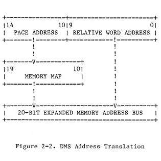
The software has access to three registers on the DMSB, Latch A, Latch B and Latch C. Latch C is a five bit register which is compared with the processor address bits 14 to 10. For addresses below the Latch C value the contents of Latch A is used to calculate the extended address value and for processor addresses equal to or greater than the Latch C value then Latch B is used in the extended address calculation. Latch A and B are used in the extended address calculation to provide a 2k oct page address, bits 19 to 10. See below:
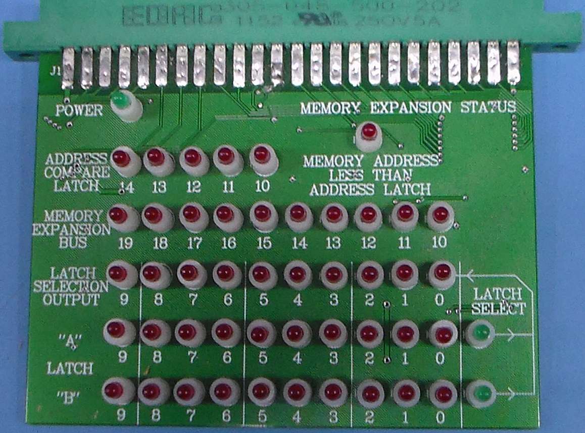
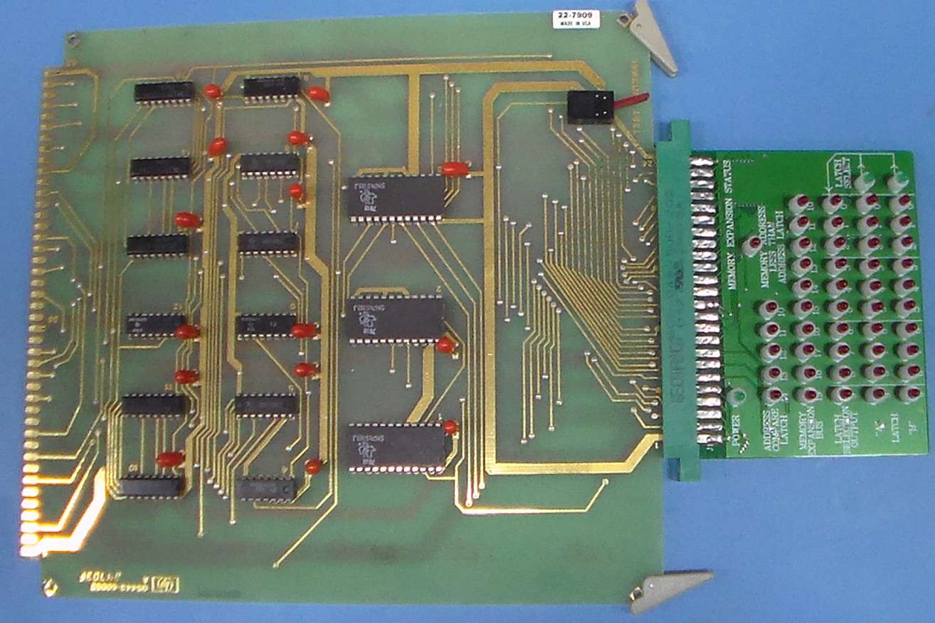
This simple DMS does not allow you to directly read back the latch settings and therefore you can't find out which part of memory is switched in at any given moment unless you single step through the software and read the memory used to hold the current settings, this memory changes depending on which software is running. This next image is of the Dynamic Mapping System Board (DMSB) p/n 05443-60057, when HP designed this board they included a connector on the top of the board which provided all of the necessary status signals so that you can see all the latch settings, the memory expansion bus bits 19-10, the M-Bus bits 14-10, and the state of the Latch A/B multiplexer.
I have designed a status indicator PCB that plugs into the DMSB allowing me to verify that the latches are set correctly by any software I've written. Below is the DMSB with the status PCB connected.
This DMSB requires two special instructions which are in the microcode ROMs supplied, I guess these instructions were only used in the 5420A and 5423A systems as I've not found any reference to them in any general documentation for the HP21MX or HP1000 computers.
These instructions are 105573 oct and 105574 oct, 105573 sets Latch A and Latch C while 105574 sets Latch B. Latch A or register A0 is the start address of memory segment 1, this is a 10 bit register so the start address is actually a 2k octal (1024 dec) page number. Latch C or register AL is the memory segment length in 2k octal pages, this register is five bits is in length and is compared with processor address bits 10-14 to determine which memory segment is selected. Latch B or register B0-AL is a 10 bit register giving the page address of memory segment 2 where the data for Latch B is the page address minus the segment length AL.
So for base memory addresses where M-Bus bits 10-14 are less than the AL register memory segment 1 is selected and where M-Bus bits 10-14 are greater then or equal to the AL register then memory segment 2 is selected. Depending whether register A0 or B0-AL is selected these 10 bits are used as bits 10-19 and are added to M-Bus bits 10-14 using a full look-ahead carry adder. Bits 0-9 from M-Bus and the result from the adder makes up the Memory Expansion Bus (ME-Bus) bits 0-19.
Both of these DMS set up instructions require the CPU A-register to be loaded with a pointer to the memory location containing either the A0 or B0-AL register data and for the 105573 instruction the AL register data must be in the next consecutive location after the A0 register data.
Earlier 48k word versions of the HP5420A used a different bank switching method. These instruments had 16k words of memory fixed in the address range 000000-037777 oct and for the address range 040000-077777 oct there were two 16k word banks which were called Leg-A and Leg-B. To switch in Leg-A you execute instruction XAM 105522 oct and for Leg-B you execute XBM 105526 oct. The later 5420As and 5423As have these instructions implemented for backward compatibility but the memory is selected via the DMS.
Here is a closeup of my DMS Status PCB.