 |
Front Panel |
Download Documents
Front Panel SchematicWhat is the goal of this project?
The primary purpose of this project has been to save the system software used by the the 5420A/B and 5423A. Restoration of the equipment has been a key part of the project but connection of the system to a modern PC so that the system software could be stored on a medium with higher reliabilty than the original DC-100A tape cartridges is the first major step.
When I first started thinking about how to approach the issue of saving the system software I had to learn as much as I could about these systems and the 21MX series of processors. From this a list of requirements was made.
| 1. | Do not want to make any hardware modifications. |
| 2. | Do not want to use the interrupt system in case it causes confilcts. |
| 3. | Memory usage is to be minimal and any data destroyed by its use has to be restored. |
| 4. | Use of standard I/O board will mean that additional software is required and there many not be sufficient memory in the system. |
| 5. | The ability to set addresses, read and write data, execute software, etc. |
| 6. | The ability to capture system software prior to execution and therefore it not be initialised. |
| 7. | Any data captured has to be validated as correct. |
| 8. | Bank switching of memory is required so all memory can read or written. |
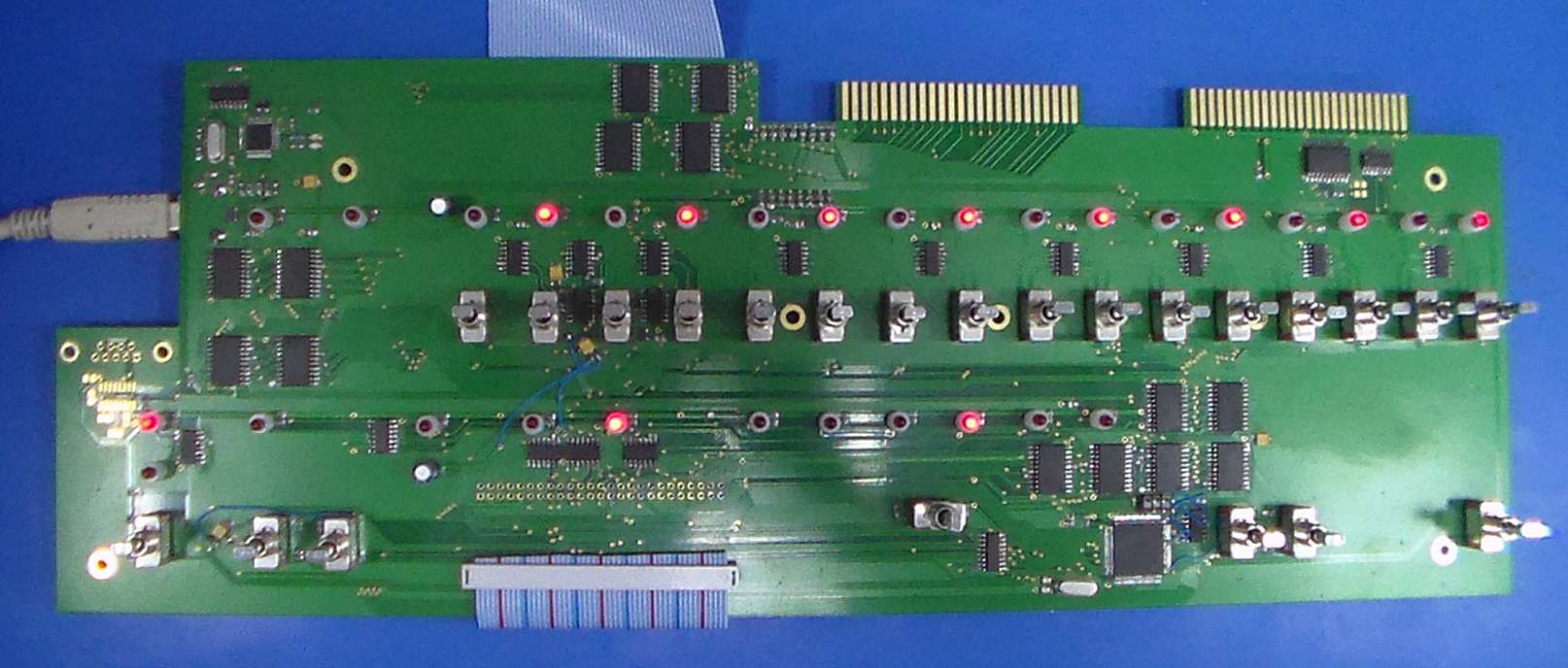
These requirements pointed in the direction of making a front panel, a traditional LED and switch job. To interface back to a host PC circuitry was added to the original HP design, this included an ATMega128 capable of controlling all of the front panel functions and a USB chip for connection to a PC. Further, a connector is available on the front panel of the equipment and the system knows when a front panel is connected.
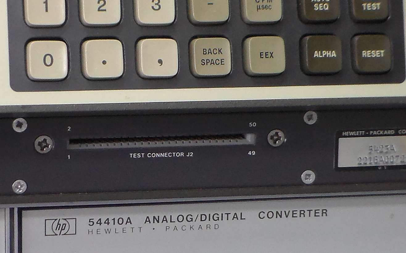
The J2 connector is for the 21MX front panel.
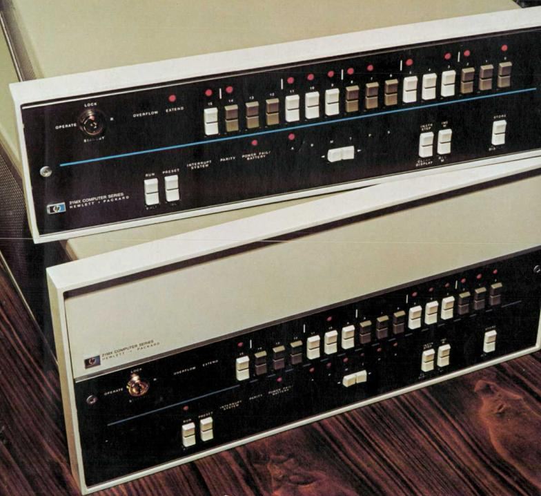
Below you can see the original HP 21MX front panels these allow the operator to display and write to registers and memory. Also the operator can run and halt software loaded in memory plus error conditions and status are displayed on special LEDs.
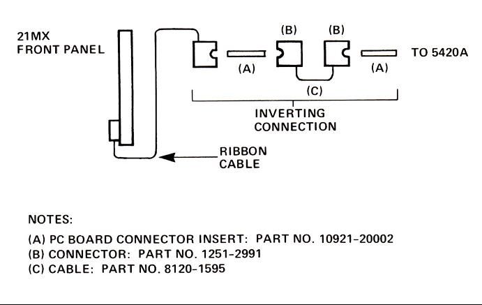
The J2 connector on the 5420A/B and 5423A systems cannot connect directly with a 21MX front panel, the wiring was swapped over, I have no idea why HP swapped these J2 connections but the image below from the manual shows how the front panel should be connected. On my version of the front panel two sets of connectors were included so the use of multiple adaptors is not required.
The HP front panel used though hole ics because of when it was designed, fortunately I didn't have that constraint so using surface mount componentry simplified the board layout and there was plenty of extra space for the additional componentry.
Logic Families
Various 74xx series logic families were used in the circuit based on the interface requirements of the 21MX processor and on issues that arose during testing. Generally all of the bus interface circuitry required 74Sxx logic to meet drive and speed requirements, so 74Sxx parts were used in those parts of the circuit. Other circuitry only required standard 74xx or 74LSxx type devices, 74ACTxx and 74ALSxx were the most readily available in SO packages. Further, I thought that 74ACTxx devices would be a good choice for low power consumption and for the most part this assumption was valid.
When first testing the board however, the current draw was higher than I expected and the LEDs would not hold in the new state if the bit state was toggled. Each bit of the 16 bit data and 15 bit address buses are latched by a simple two NAND gate flip-flop, after checking the voltage level of a logic "1" for various families and I suspected that the ACT family would not work well in this type of circuit and that there possibly was some latchup occurring. After changing out the 74ACT00s for 74ALS00s in the bit latch circuits they began to function correctly allowing the bit state to be set and the power consumption reduced to half. A quick handy reference for comparison of voltages specifications between different logic families can be found here.
21MX Front Panel with USB Interface.
Switch Debouncing
Data input via the front panel is the switches, switches need to be debounced and usually as software time constant is used as part of the debounce function. Fortunately in this case a capacitor was used, I say fortunately because one goal of this design was to communicate with the processor at a higher data rate than that of manually toggling switches. The idea here was to disable the debounce capacitor under software control so that when host PC was communicating with the 21MX processor "high" data rates could be used. However, when I designed the front panel PCB I forgot to add this feature so the board had to be modified when it was received from the PCB manufacturer. When testing data transfer rates with the switch debouce disabled the maximum data rate was dependent on function type, like any peripheral on the 21MX the front panel does require some code to function and in this case micro-code was used. Therefore, when executing a given function there was a finite execution time. These times were measured and incorporated into the code for the ATMega128.
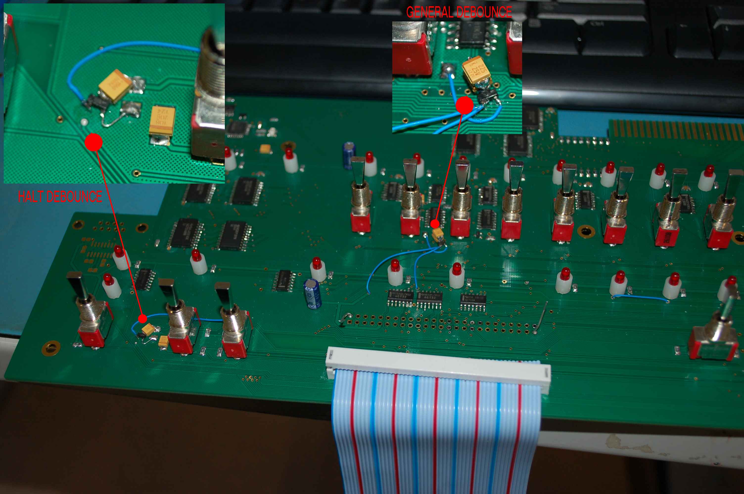
General and Halt debounce capacitors with control MOSFETs which switch the debounce function ON or OFF.
Faulty Data and Logic Families
While working in the code for the ATMega128 and the VB code running on the PC there were certain data patterns that would not correctly set the certain bits on the front panel display. Initially I couldn't see why I was having this issue and this was one of those types of probems that you put aside for a while then come back to with hopefully a fresh approach. One clue here was that the origin of the faulty data was data writes from the ATMega128 to the bit latches and the tri-state buffer was in 74Sxx logic the same type of buffer used to connect back into the 21MX processor.
Not being able to see an obvious way forward I re-read the HP documentation and I found a short paragraph relating to the "display reset". Basically the data buffers which write data to the bit latches are incapable of resetting the latch ie setting a logic "0" (LED off) as the drive to the latch is inverted this means a logic "1" into the latch displays a logic "0". To fix this issue HP had a an extra input to each latch which could clear the latch prior to it being written with new data. So my first thought was to provide a "display reset" from the ATMega128 so HP's technique could be replicated. However, I had run out of I/O lines on ATMega128, well not quite there was one left, but I didn't want modify the board if it wasn't necessary. While pondering this issue my thoughts went back to the issue I had previously had with 74ACTxx and as the output voltage for a logic "1" is 4.7V instead of 3.3V for 74Sxx I suspected that the ACT family my be able to drive a logic "1" into the latch making it change state where the 74Sxx part conuld not. The 74Sxx data buffers were changed for 74ACTxx parts and bingo it worked without the need to pre-clear the latches.
Further, as data intergrity was more important than speed a data verification step was added with automatic retries and an error returned after the retry limit is exceeded.
Apart from the embedded code in the ATMega128, a Windows app was written to control the front panel, provide storage for the control software in the 5420A/B and 5423A, and then it has grown as I have required new functions for the restoration project.